
Exploring the Art of Wafer Packing: A Comprehensive Guide
The Beauty and Complexity of Wafer Packing
Welcome to the fascinating world of wafer packing! In semiconductor manufacturing, the process of packing wafers is crucial for ensuring the integrity and quality of the delicate semiconductor components. Let’s delve into the art and science behind wafer packing and why it holds a significant role in the semiconductor industry.
The Importance of Proper Wafer Packing
Wafer packing is not just about placing wafers into containers; it involves precision, care, and attention to detail. The primary purpose of wafer packing is to protect the wafers from contamination, physical damage, and exposure to harmful environmental factors. Additionally, proper packing helps in maintaining the cleanliness of the wafers and prevents any potential defects that could affect their performance.
Types of Wafer Packing Materials
There are several materials used for wafer packing, including plastic trays, gel packs, and vacuum-sealed containers. Each type of packing material serves a specific purpose and is chosen based on the requirements of the semiconductor manufacturer. Plastic trays are commonly used for transporting wafers within the manufacturing facility, while gel packs provide protection against humidity and moisture during shipping.
The Process of Wafer Packing
The process of wafer packing involves several steps, starting from inspecting the wafers for defects to placing them carefully into the packing material. Cleanroom conditions are essential during the packing process to ensure that no contaminants come in contact with the wafers. Once packed, the wafers are sealed and labeled for identification purposes.
Challenges in Wafer Packing
Despite the advancements in wafer packing technology, there are still challenges faced by semiconductor manufacturers. Issues such as electrostatic discharge, thermal stress, and transportation damage can impact the quality of the wafers. Overcoming these challenges requires continuous innovation and strict adherence to quality control measures.
Future Trends in Wafer Packing
As semiconductor technology continues to evolve, so do the methods and materials used in wafer packing. Innovations such as smart packaging solutions, biodegradable materials, and advanced monitoring systems are shaping the future of wafer packing. These developments aim to enhance the efficiency, reliability, and sustainability of wafer packing processes.
Conclusion
Wafer packing is a critical step in semiconductor manufacturing, ensuring the safe and secure transportation of delicate wafers from production to assembly. By understanding the complexities and challenges involved in wafer packing, semiconductor manufacturers can optimize their processes and deliver high-quality products to meet the demands of the industry.


-
01
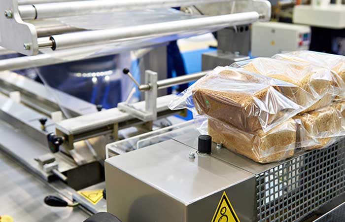
How do I choose the right speed for a toas bread packaging line to avoid crushing soft loaves?
22-06-2026 -
 02
02Packaging Machinery: Beyond Sealing, Driving an Efficient, Smart, and Sustainable Future
21-01-2026 -
 03
03Automatic Tray Loading and Packaging Equipment: Boost Efficiency to 160 Bags/Minute
21-11-2025 -
 04
04Automatic Soap Packaging Machine: Boost Productivity with 99% Qualification Rate
21-11-2025 -
 05
05A Deep Dive into Automatic Toast Processing and Packaging System
18-11-2025 -
06
The Future of Bakery Production: Automated Toast Processing and Packaging System
18-11-2025 -
 07
07Reliable Food Packaging Solutions with China Bread, Candy, and Biscuit Machines
11-10-2025 -
 08
08High-Performance Automated Food Packaging Equipment for Modern Production
11-10-2025 -
09
Reliable Pillow Packing Machines for Efficient Packaging Operations
11-10-2025 -
 10
10Advanced Fully Automatic Packaging Solutions for Efficient Production
11-10-2025
