
Revolutionary Wafer Packaging Solutions for the Future

The Future of Wafer Packaging: Innovations and Sustainable Solutions
In the contemporary landscape of electronics and semiconductor manufacturing, wafer packaging is undergoing a revolutionary transformation. The demand for smaller, faster, and more efficient electronic devices has led to an increased focus on enhancing wafer packaging solutions to meet these evolving industry demands.
Introduction to Wafer Packaging
Wafer packaging is a critical process in the semiconductor industry where individual silicon chips are embedded and interconnected to create functional microelectronic devices. Traditional packaging methods have often faced challenges in terms of size, efficiency, and environmental impact.
The Need for Innovation
With the rapid advancements in technology and the rise of IoT devices, there is a growing need for innovative wafer packaging solutions that can deliver increased performance, reduced footprint, and enhanced sustainability. Companies are now exploring cutting-edge approaches such as 3D packaging, embedded wafer-level optics, and fan-out wafer-level packaging.
Sustainable Packaging Solutions
As the world shifts towards sustainability, the semiconductor industry is also focusing on eco-friendly wafer packaging solutions. Biodegradable packaging materials, energy-efficient manufacturing processes, and recyclable packaging designs are some of the key trends shaping the future of wafer packaging.
Advancements in Wafer-Level Packaging
Wafer-level packaging technologies are rapidly evolving to address the demands of next-generation electronic devices. From advanced interconnect technologies to wafer-level fan-out packaging, these innovations are enabling manufacturers to create smaller, faster, and more power-efficient devices.
The Role of AI in Wafer Packaging
Artificial intelligence is playing a crucial role in optimizing wafer packaging processes. Machine learning algorithms are being utilized to improve yield rates, accelerate testing procedures, and enhance overall packaging efficiency. AI-driven wafer inspection systems are also contributing to the quality control of packaged wafers.
Conclusion
As the semiconductor industry continues to evolve, wafer packaging solutions are set to play a vital role in shaping the future of electronics manufacturing. By embracing innovation, sustainability, and advanced technologies, companies can unlock new possibilities in wafer packaging and pave the way for a more efficient and interconnected world.


-
01
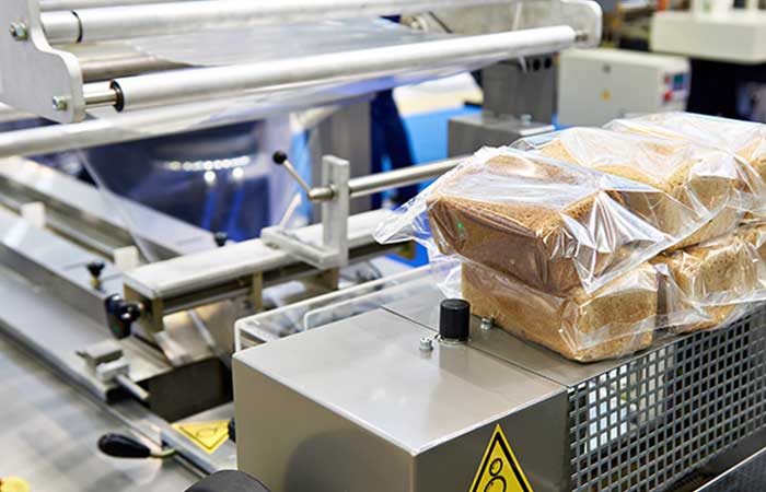
How do I choose the right speed for a toas bread packaging line to avoid crushing soft loaves?
22-06-2026 -
 02
02Packaging Machinery: Beyond Sealing, Driving an Efficient, Smart, and Sustainable Future
21-01-2026 -
 03
03Automatic Tray Loading and Packaging Equipment: Boost Efficiency to 160 Bags/Minute
21-11-2025 -
 04
04Automatic Soap Packaging Machine: Boost Productivity with 99% Qualification Rate
21-11-2025 -
 05
05A Deep Dive into Automatic Toast Processing and Packaging System
18-11-2025 -
06
The Future of Bakery Production: Automated Toast Processing and Packaging System
18-11-2025 -
 07
07Reliable Food Packaging Solutions with China Bread, Candy, and Biscuit Machines
11-10-2025 -
 08
08High-Performance Automated Food Packaging Equipment for Modern Production
11-10-2025 -
09
Reliable Pillow Packing Machines for Efficient Packaging Operations
11-10-2025 -
 10
10Advanced Fully Automatic Packaging Solutions for Efficient Production
11-10-2025
