
Revolutionizing Semiconductor Packaging: The Future of Wafer Packaging Systems
Revolutionizing Semiconductor Packaging: The Future of Wafer Packaging Systems
In the realm of semiconductor manufacturing, advancements in wafer packaging systems present a transformative shift. The intricacies of wafer packaging and assembly have immense implications for the efficiency and reliability of semiconductor devices. Stay tuned as we delve into the evolving landscape of wafer packaging systems and what the future holds for this critical aspect of semiconductor production.
From conventional wire bonding techniques to cutting-edge fan-out wafer-level packaging (FOWLP) technologies, the evolution of wafer packaging systems has been rapid and revolutionary. The drive for miniaturization, increased functionality, and enhanced performance has propelled innovations in packaging methodologies, ushering in an era of unprecedented possibilities.
The integration of advanced materials, such as lead-free solder and copper pillar bumping, has significantly enhanced the thermal and electrical properties of packaged semiconductor devices. With an emphasis on reducing form factor while maintaining superior performance, wafer packaging systems have become a cornerstone of modern electronics manufacturing.
Moreover, the shift towards heterogeneous integration and 3D packaging architectures has opened up new avenues for optimizing system-level performance and functionality. By stacking multiple dies vertically and utilizing advanced interconnect technologies, wafer packaging systems enable the creation of highly compact and efficient semiconductor solutions.
As we look ahead, the convergence of AI-driven design methodologies and additive manufacturing techniques promises to further revolutionize wafer packaging systems. The adaptive nature of these technologies allows for rapid prototyping and customization, optimizing the development cycle and accelerating time-to-market for semiconductor products.
In conclusion, the future of wafer packaging systems is poised to redefine the boundaries of semiconductor innovation. By embracing cutting-edge technologies and novel packaging paradigms, manufacturers can unlock new levels of performance, efficiency, and reliability in semiconductor devices. Join us on this journey of transformation as we explore the limitless possibilities of wafer packaging systems in shaping the future of electronics.


-
01
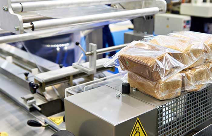
How do I choose the right speed for a toas bread packaging line to avoid crushing soft loaves?
22-06-2026 -
 02
02Packaging Machinery: Beyond Sealing, Driving an Efficient, Smart, and Sustainable Future
21-01-2026 -
 03
03Automatic Tray Loading and Packaging Equipment: Boost Efficiency to 160 Bags/Minute
21-11-2025 -
 04
04Automatic Soap Packaging Machine: Boost Productivity with 99% Qualification Rate
21-11-2025 -
 05
05A Deep Dive into Automatic Toast Processing and Packaging System
18-11-2025 -
06
The Future of Bakery Production: Automated Toast Processing and Packaging System
18-11-2025 -
 07
07Reliable Food Packaging Solutions with China Bread, Candy, and Biscuit Machines
11-10-2025 -
 08
08High-Performance Automated Food Packaging Equipment for Modern Production
11-10-2025 -
09
Reliable Pillow Packing Machines for Efficient Packaging Operations
11-10-2025 -
 10
10Advanced Fully Automatic Packaging Solutions for Efficient Production
11-10-2025
