
Revolutionizing Semiconductor Tech: The Future of Wafer Level Packaging Equipment

The Future of Wafer Level Packaging Equipment: A Game Changer in Semiconductor Manufacturing
In the dynamic landscape of semiconductor technology, wafer level packaging equipment plays a pivotal role in enabling smaller, faster, and more efficient microelectronics. As industries clamor for greater performance in compact devices, the evolution of wafer level packaging has emerged as a key solution. Let’s delve into the exciting realm of wafer level packaging and explore how it is revolutionizing semiconductor manufacturing.
Wafer level packaging offers numerous advantages over traditional packaging methods. By integrating packaging processes directly onto the wafer, it reduces overall costs, improves reliability, and enhances thermal management. This streamlined approach not only boosts production efficiency but also enables the creation of ultra-compact devices with high levels of integration.
One of the breakthrough technologies driving the future of wafer level packaging is fan-out wafer-level packaging (FOWLP). FOWLP enables the assembly of multiple chips on a single wafer, leading to higher interconnect density and improved electrical performance. This advanced packaging technique is rapidly gaining traction in the industry, paving the way for cutting-edge applications such as 5G communications, artificial intelligence, and autonomous vehicles.
Furthermore, the integration of wafer level packaging with emerging technologies like chiplets and heterogeneous integration is reshaping the semiconductor landscape. Chiplets allow the modular assembly of semiconductor components, facilitating rapid prototyping and customization while reducing time-to-market. By combining chiplets with wafer level packaging, manufacturers can achieve unprecedented levels of flexibility, scalability, and performance in semiconductor design.
The evolution of wafer level packaging equipment is not just limited to hardware advancements. Innovations in software algorithms, automation, and machine learning are driving significant improvements in process control, yield optimization, and defect detection. These intelligent systems are empowering manufacturers to achieve higher throughput, lower costs, and superior quality in wafer level packaging production.
Looking ahead, the future of wafer level packaging equipment holds immense potential for transforming semiconductor manufacturing. As technology continues to advance at a rapid pace, the adoption of innovative packaging solutions will be crucial in meeting the escalating demands for smaller, faster, and more powerful devices. By embracing the latest developments in wafer level packaging, manufacturers can stay at the forefront of the industry and unlock new opportunities for growth and innovation.


-
01
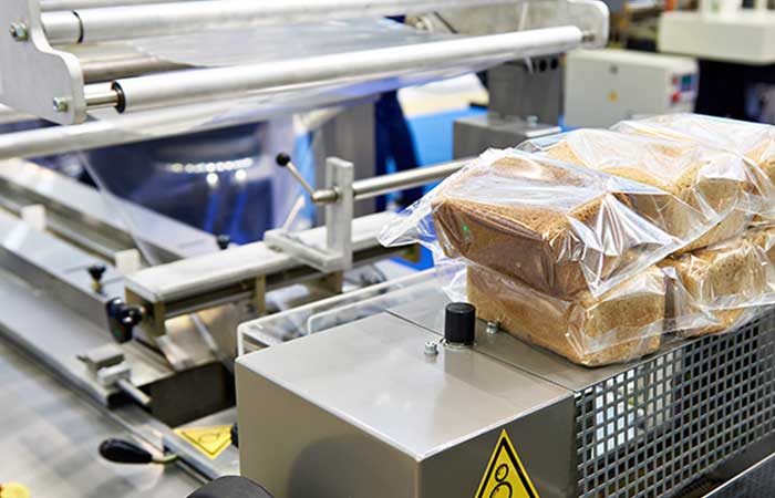
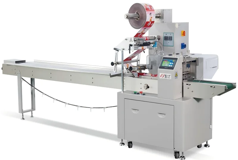
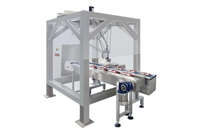
How do I choose the right speed for a toas bread packaging line to avoid crushing soft loaves?
22-06-2026 -
 02
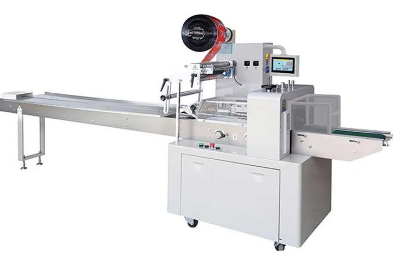
02Packaging Machinery: Beyond Sealing, Driving an Efficient, Smart, and Sustainable Future
21-01-2026 -
 03
03Automatic Tray Loading and Packaging Equipment: Boost Efficiency to 160 Bags/Minute
21-11-2025 -
 04
04Automatic Soap Packaging Machine: Boost Productivity with 99% Qualification Rate
21-11-2025 -
 05
05A Deep Dive into Automatic Toast Processing and Packaging System
18-11-2025 -
06
The Future of Bakery Production: Automated Toast Processing and Packaging System
18-11-2025 -
 07
07Reliable Food Packaging Solutions with China Bread, Candy, and Biscuit Machines
11-10-2025 -
 08
08High-Performance Automated Food Packaging Equipment for Modern Production
11-10-2025 -
09
Reliable Pillow Packing Machines for Efficient Packaging Operations
11-10-2025 -
 10
10Advanced Fully Automatic Packaging Solutions for Efficient Production
11-10-2025
