Revolutionizing Semiconductor Transportation: The Art of Wafer Packing
The Art of Wafer Packing
Wafer packing is an essential process in the semiconductor industry. It involves carefully packaging delicate silicon wafers, which are the foundation of microelectronics, for safe transportation and storage. The semiconductor industry relies heavily on wafer packing to ensure that these crucial components remain intact and undamaged throughout their journey from fabrication facilities to assembly plants.
One of the key challenges in wafer packing is to minimize any potential damage to the wafers during transportation. Silicon wafers are extremely fragile and prone to breakage if not handled with care. This is why specialized packaging materials and techniques are used to protect the wafers from external shocks and environmental factors.
Several factors need to be considered when designing wafer packing solutions. These include the size and thickness of the wafers, the distance they need to travel, and the conditions they will be exposed to during transit. Different types of packaging materials, such as foam inserts, antistatic bags, and protective casings, are used to provide varying levels of protection to the wafers.
Technological advancements have led to the development of innovative wafer packing solutions that offer enhanced protection and efficiency. For example, some companies have started using vacuum-sealed packaging to create a controlled environment around the wafers, preventing contamination and oxidation. Others have incorporated shock-absorbing materials into their packaging to reduce the risk of breakage.
Furthermore, sustainability is becoming a key consideration in wafer packing. As the industry moves towards environmentally friendly practices, there is a growing emphasis on using recyclable and biodegradable materials in packaging. Companies are exploring new ways to minimize waste and reduce the environmental impact of their packaging processes.
The Future of Wafer Packing
Looking ahead, the future of wafer packing is likely to be shaped by advancements in materials science and automation. Researchers are exploring the use of novel materials that offer superior protection while remaining lightweight and cost-effective. Automation technologies, such as robotic packing systems, are also being developed to streamline the packing process and improve efficiency.
Overall, wafer packing plays a critical role in ensuring the integrity and reliability of semiconductor components. By investing in innovative packing solutions and sustainable practices, the industry can continue to drive forward technological progress and meet the increasing demand for high-performance microelectronics.
Stay tuned for more updates on the latest developments in wafer packing and semiconductor transportation!


-
 01
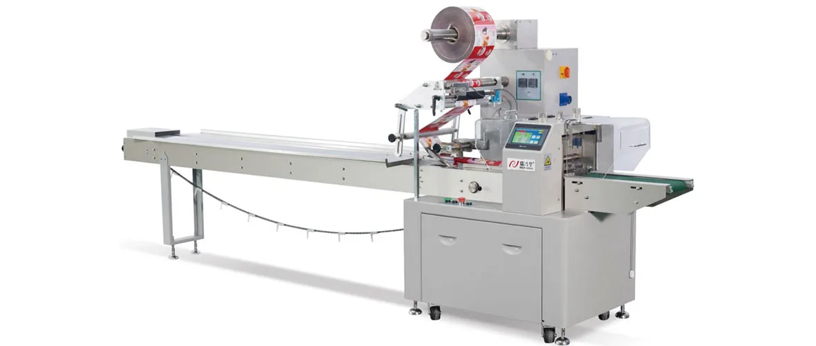
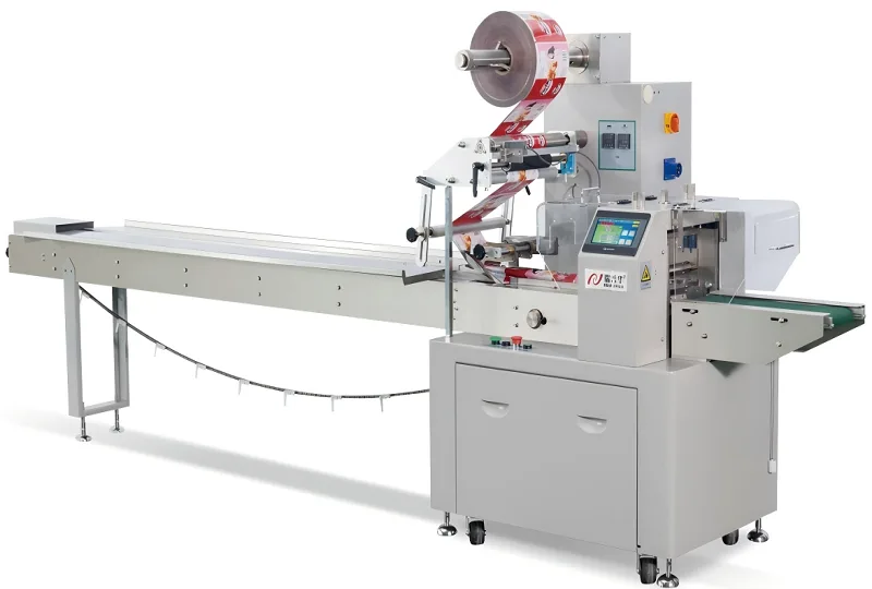
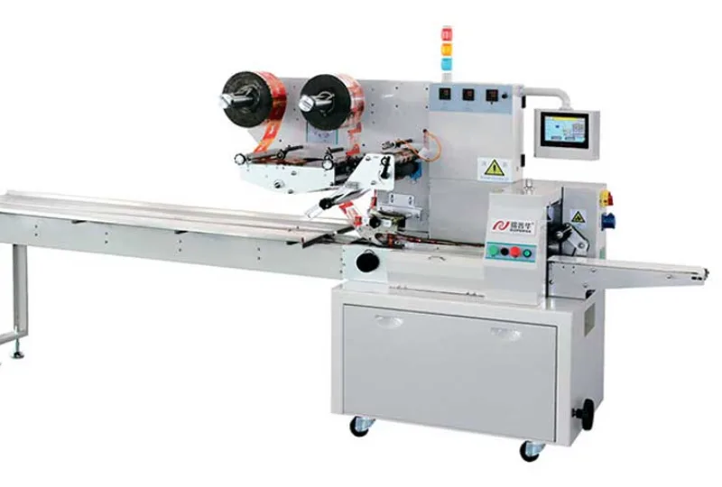
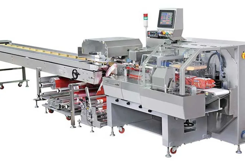
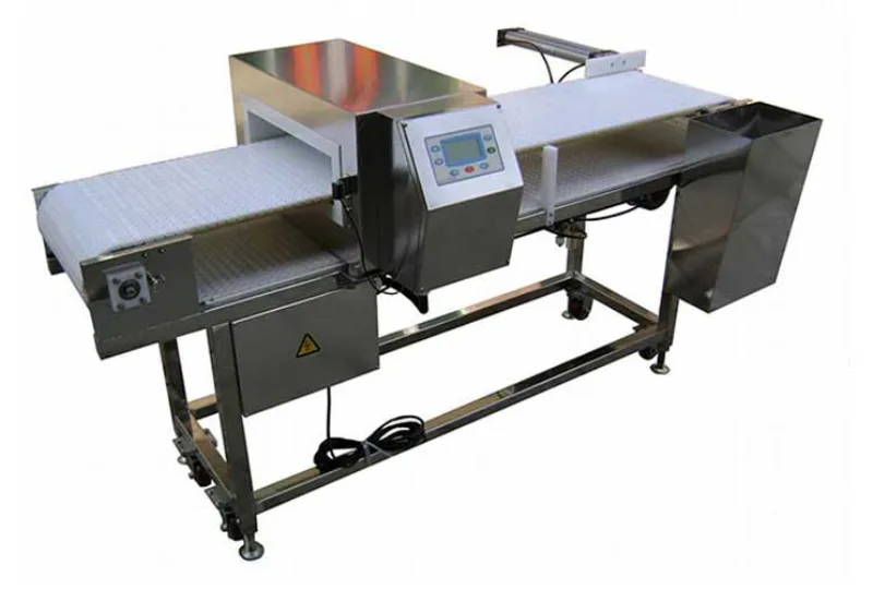
01Packaging Machinery: Beyond Sealing, Driving an Efficient, Smart, and Sustainable Future
21-01-2026 -
 02
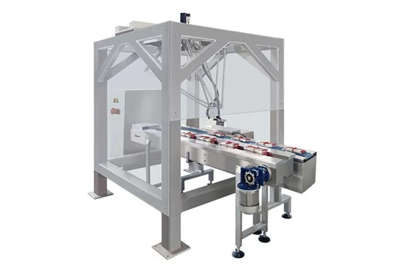
02Automatic Tray Loading and Packaging Equipment: Boost Efficiency to 160 Bags/Minute
21-11-2025 -
03
Automatic Soap Packaging Machine: Boost Productivity with 99% Qualification Rate
21-11-2025 -
04
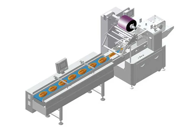
A Deep Dive into Automatic Toast Processing and Packaging System
18-11-2025 -
05
The Future of Bakery Production: Automated Toast Processing and Packaging System
18-11-2025 -
06
Reliable Food Packaging Solutions with China Bread, Candy, and Biscuit Machines
11-10-2025 -
07
High-Performance Automated Food Packaging Equipment for Modern Production
11-10-2025 -
08
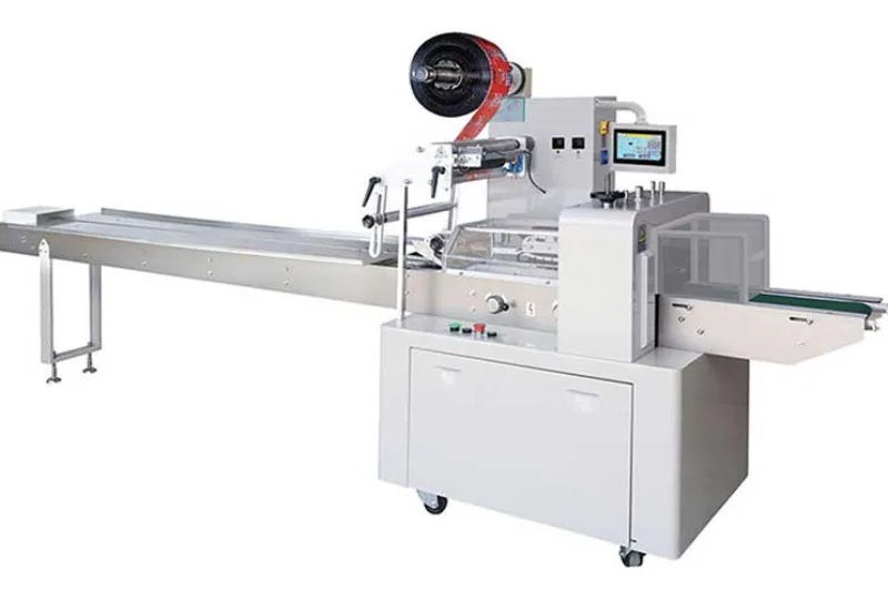
Reliable Pillow Packing Machines for Efficient Packaging Operations
11-10-2025 -
09
Advanced Fully Automatic Packaging Solutions for Efficient Production
11-10-2025 -
10
Efficient Automatic Food Packaging Solutions for Modern Production
11-10-2025