
Revolutionizing Wafer Packaging: A Deep Dive into Advanced Solutions
Revolutionizing Wafer Packaging: A Deep Dive into Advanced Solutions
In the dynamic realm of semiconductor manufacturing, wafer packaging stands as a critical phase that wields a profound impact on the final product. Over the years, advancements in technology have revolutionized the way we approach wafer packaging, ushering in a new era of efficiency and reliability. Let’s explore some of the cutting-edge solutions that are reshaping the landscape of wafer packaging.
The Rise of Fan-Out Wafer-Level Packaging
One of the most notable advancements in wafer packaging is the increasing adoption of fan-out wafer-level packaging (FOWLP). This innovative approach offers a myriad of benefits, including enhanced thermal performance, reduced form factor, and increased density. By redistributing the traditional I/O connections to the periphery of the chip, FOWLP enables higher levels of integration and improved electrical performance.
Encapsulating Wafer-Level Chip Scale Packaging
Another fascinating development in wafer packaging is the emergence of wafer-level chip scale packaging (WLCSP). This technology eliminates the need for traditional packaging materials by directly encapsulating the chip at the wafer level. With its compact size and minimal footprint, WLCSP offers significant cost reductions and improved electrical performance for a wide range of applications.
Exploring the Potential of Through-Silicon Vias
Through-silicon vias (TSVs) represent a groundbreaking innovation in wafer packaging, enabling vertical interconnects that traverse the thickness of the silicon wafer. By facilitating direct connections between multiple stacked dies, TSVs unlock new possibilities for 3D integration and system-level miniaturization. This technology holds immense promise for enhancing performance and enabling more complex semiconductor architectures.
Integrating Advanced Materials for Enhanced Reliability
As the demand for higher performance and reliability continues to rise, the incorporation of advanced materials in wafer packaging has become paramount. From underfill materials to mold compounds, each component plays a crucial role in ensuring the longevity and robustness of the final product. By leveraging innovative materials with superior thermal and mechanical properties, manufacturers can enhance the durability and reliability of their semiconductor devices.
Optimizing Post-Wafer Processing for Superior Yield
Post-wafer processing plays a critical role in determining the overall yield and quality of packaged semiconductor devices. By implementing advanced techniques such as wafer thinning, dicing, and backside grinding, manufacturers can optimize the packaging process for maximum efficiency and yield. These strategies not only improve the overall cost-effectiveness of wafer packaging but also contribute to the development of high-performance, reliable integrated circuits.
Embracing the Future of Wafer Packaging
As we delve deeper into the realm of wafer packaging, it is evident that innovation is driving the industry towards unprecedented levels of performance and efficiency. By embracing cutting-edge technologies and materials, manufacturers can unlock new possibilities for semiconductor packaging and propel the field towards a future defined by advancements in miniaturization, integration, and reliability.


-
01
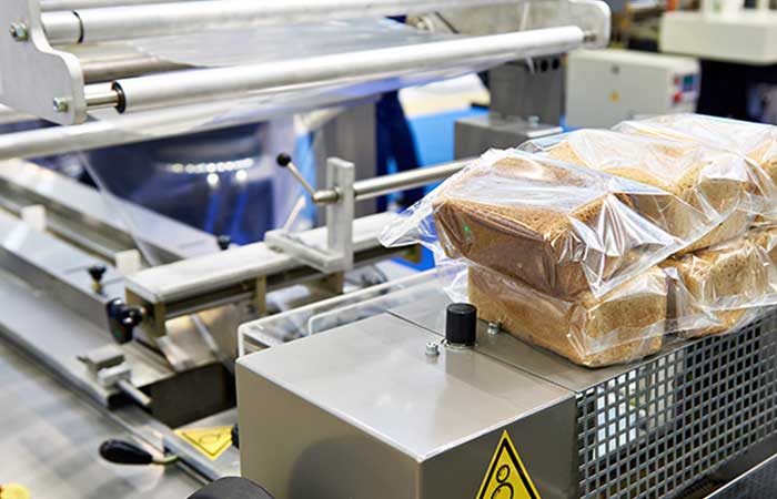
How do I choose the right speed for a toas bread packaging line to avoid crushing soft loaves?
22-06-2026 -
 02
02Packaging Machinery: Beyond Sealing, Driving an Efficient, Smart, and Sustainable Future
21-01-2026 -
 03
03Automatic Tray Loading and Packaging Equipment: Boost Efficiency to 160 Bags/Minute
21-11-2025 -
 04
04Automatic Soap Packaging Machine: Boost Productivity with 99% Qualification Rate
21-11-2025 -
 05
05A Deep Dive into Automatic Toast Processing and Packaging System
18-11-2025 -
06
The Future of Bakery Production: Automated Toast Processing and Packaging System
18-11-2025 -
 07
07Reliable Food Packaging Solutions with China Bread, Candy, and Biscuit Machines
11-10-2025 -
 08
08High-Performance Automated Food Packaging Equipment for Modern Production
11-10-2025 -
09
Reliable Pillow Packing Machines for Efficient Packaging Operations
11-10-2025 -
 10
10Advanced Fully Automatic Packaging Solutions for Efficient Production
11-10-2025
