
Wafer Packing Solutions: The Ultimate Guide to Precision Packaging for Semiconductor Wafers
Understanding Wafer Packing: The Critical Role in Semiconductor Manufacturing
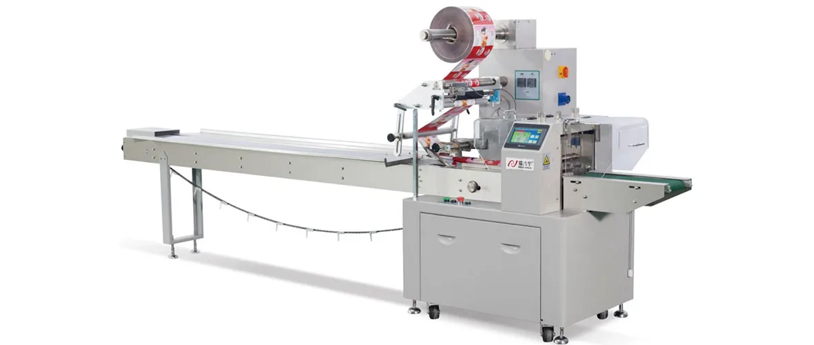
Wafer packing is a specialized process that ensures the safe handling, storage, and transportation of semiconductor wafers—thin slices of crystalline silicon used in the production of integrated circuits (ICs). As wafers are extremely sensitive to physical damage, contamination, and electrostatic discharge (ESD), proper packing is essential to maintain their integrity throughout the supply chain.
Key Components of Wafer Packing Systems
Modern wafer packing systems typically include anti-static materials, humidity control mechanisms, and shock-absorbing structures. These components work together to protect wafers from environmental factors that could compromise their performance. For example, anti-static bags prevent ESD, which can damage delicate electronic components on the wafer surface.
Industry Standards for Wafer Packing
The semiconductor industry adheres to strict standards for wafer packing, such as those set by the Semiconductor Equipment and Materials International (SEMI). These standards specify requirements for materials, design, and testing to ensure consistency and reliability across the supply chain.
Advanced Technologies in Wafer Packing
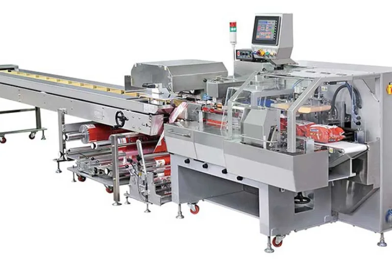
Recent advancements in wafer packing technology have focused on automation, precision, and sustainability. Automated packing systems use robotics and machine vision to handle wafers with minimal human intervention, reducing the risk of contamination and improving efficiency.
Automated Wafer Packing Systems
Automated systems can perform tasks such as wafer loading, alignment, and sealing with high precision. These systems often integrate with other manufacturing processes, creating a seamless workflow that enhances productivity. For instance, robotic arms can place wafers into packing containers with sub-millimeter accuracy, ensuring optimal protection.
Sustainable Wafer Packing Solutions
As environmental concerns grow, the industry is moving toward sustainable packing materials. Biodegradable and recyclable materials are being developed to reduce the environmental impact of wafer packing. Additionally, reusable packing containers are becoming more common, further minimizing waste.
Choosing the Right Wafer Packing Solution
Selecting the appropriate wafer packing solution depends on several factors, including wafer size, material, and transportation requirements. It is crucial to work with a provider that understands the unique needs of the semiconductor industry and can offer customized solutions.
Customization Options for Wafer Packing
Custom packing solutions can be tailored to specific wafer dimensions, storage conditions, and transportation modes. For example, wafers used in high-temperature applications may require heat-resistant packing materials, while those transported over long distances need enhanced shock protection.
Partnering with a Reliable Wafer Packing Provider
When choosing a wafer packing provider, it is important to consider their experience, technical expertise, and commitment to quality. A reliable provider will offer comprehensive support, from design and testing to implementation and maintenance, ensuring that your wafers are protected throughout their lifecycle.
Future Trends in Wafer Packing
The future of wafer packing is shaped by emerging technologies such as artificial intelligence (AI) and the Internet of Things (IoT). AI-powered systems can optimize packing processes in real-time, while IoT devices can monitor environmental conditions during transportation, providing valuable data for quality control.
AI and Machine Learning in Wafer Packing
AI algorithms can analyze data from packing processes to identify inefficiencies and predict potential issues. For example, machine learning models can detect patterns in packing errors, allowing for proactive adjustments to improve performance.
IoT-Enabled Wafer Packing Systems
IoT devices embedded in packing containers can track parameters such as temperature, humidity, and vibration. This data can be transmitted to a central system, enabling real-time monitoring and ensuring that wafers are stored and transported under optimal conditions.
At Ruipuhua Machinery, we specialize in providing high-quality wafer packing solutions that meet the rigorous demands of the semiconductor industry. Our advanced systems are designed to protect your wafers from damage and contamination, ensuring their performance and reliability. Contact us today to learn more about our customized packing solutions and how we can help you optimize your semiconductor manufacturing process.


-
 01
01Packaging Machinery: Beyond Sealing, Driving an Efficient, Smart, and Sustainable Future
21-01-2026 -
 02
02Automatic Tray Loading and Packaging Equipment: Boost Efficiency to 160 Bags/Minute
21-11-2025 -
 03
03Automatic Soap Packaging Machine: Boost Productivity with 99% Qualification Rate
21-11-2025 -
 04
04A Deep Dive into Automatic Toast Processing and Packaging System
18-11-2025 -
05
The Future of Bakery Production: Automated Toast Processing and Packaging System
18-11-2025 -
 06
06Reliable Food Packaging Solutions with China Bread, Candy, and Biscuit Machines
11-10-2025 -
 07
07High-Performance Automated Food Packaging Equipment for Modern Production
11-10-2025 -
08
Reliable Pillow Packing Machines for Efficient Packaging Operations
11-10-2025 -
 09
09Advanced Fully Automatic Packaging Solutions for Efficient Production
11-10-2025 -
 10
10Efficient Automatic Food Packaging Solutions for Modern Production
11-10-2025
