
Challenges and Solutions in Wafer Packaging Automation
In the rapidly evolving microelectronics industry, wafer packaging plays a critical role in protecting and enhancing semiconductor devices. The miniaturization of integrated circuits (ICs) has propelled the demand for high-precision and efficient wafer packaging automation solutions. However, this relentless pursuit of smaller, faster, and more complex devices poses significant challenges.
Challenges:
Ultrafine Pitch Interconnects: With the advent of advanced packaging technologies like fan-out wafer-level packaging (FOWLP), sub-micron interconnect pitches create challenges in ensuring accurate and reliable connections.
Complex Design Geometries: The emergence of heterogeneous integration and system-in-package (SiP) designs introduces complex device shapes and packaging requirements.
Throughput and Yield: Mass production of complex devices necessitates high throughput and yield, putting immense pressure on automation systems.
Quality Control: The stringent quality requirements of semiconductor packaging demand rigorous inspection and testing throughout the process.
Solutions:
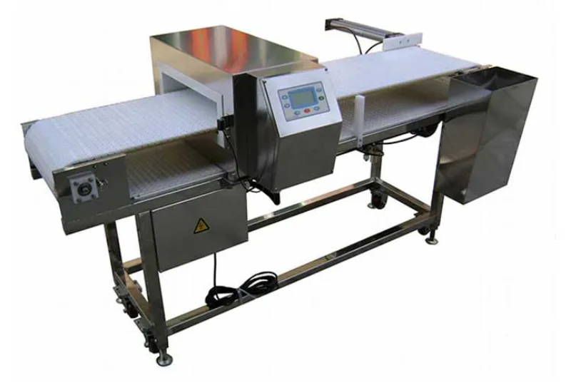
Precision Equipment: Advanced robotics, vision systems, and alignment technologies enable precise and repeatable handling of wafers and devices.
Advanced Materials: Novel materials such as graphene and ultra-thin copper allow for low-resistance interconnects and enhanced device performance.
Intelligent Fault Detection: AI-powered systems continuously monitor and detect process anomalies, reducing downtime and improving yield.
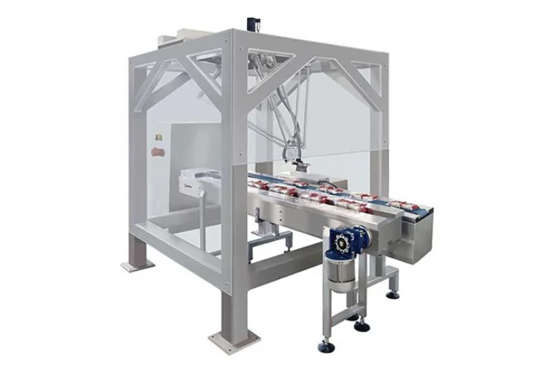
Automation Integration: Seamless integration of automation modules, including die bonding, wire bonding, encapsulation, and testing, optimizes efficiency and reduces cycle time.
Industry Collaboration: Partnerships between industry players foster innovation and advance the development of cutting-edge packaging solutions.
By addressing these challenges, wafer packaging automation empowers manufacturers to produce high-quality, high-performance devices at scale. These solutions enhance profitability, reduce time-to-market, and pave the way for the next generation of microelectronic devices.
In conclusion, the challenges in wafer packaging automation are met with innovative solutions that push the boundaries of manufacturing technology. As the industry continues to evolve, continued advancements in automation will unlock the full potential of semiconductor packaging and shape the future of next-generation electronics.


-
01
How do I choose the right speed for a toas bread packaging line to avoid crushing soft loaves?
22-06-2026 -
 02
02Packaging Machinery: Beyond Sealing, Driving an Efficient, Smart, and Sustainable Future
21-01-2026 -
 03
03Automatic Tray Loading and Packaging Equipment: Boost Efficiency to 160 Bags/Minute
21-11-2025 -
 04
04Automatic Soap Packaging Machine: Boost Productivity with 99% Qualification Rate
21-11-2025 -
 05
05A Deep Dive into Automatic Toast Processing and Packaging System
18-11-2025 -
06
The Future of Bakery Production: Automated Toast Processing and Packaging System
18-11-2025 -
 07
07Reliable Food Packaging Solutions with China Bread, Candy, and Biscuit Machines
11-10-2025 -
 08
08High-Performance Automated Food Packaging Equipment for Modern Production
11-10-2025 -
09
Reliable Pillow Packing Machines for Efficient Packaging Operations
11-10-2025 -
 10
10Advanced Fully Automatic Packaging Solutions for Efficient Production
11-10-2025
