How Wafer Packaging Lines Enhance Production Efficiency
With the ever-increasing demand for electronic devices, the semiconductor industry is facing tremendous pressure to optimize production processes and increase efficiency. Wafer packaging lines play a crucial role in this regard by transforming individual semiconductor wafers into functional integrated circuits (ICs) ready for use in electronic devices.
Automated Material Handling
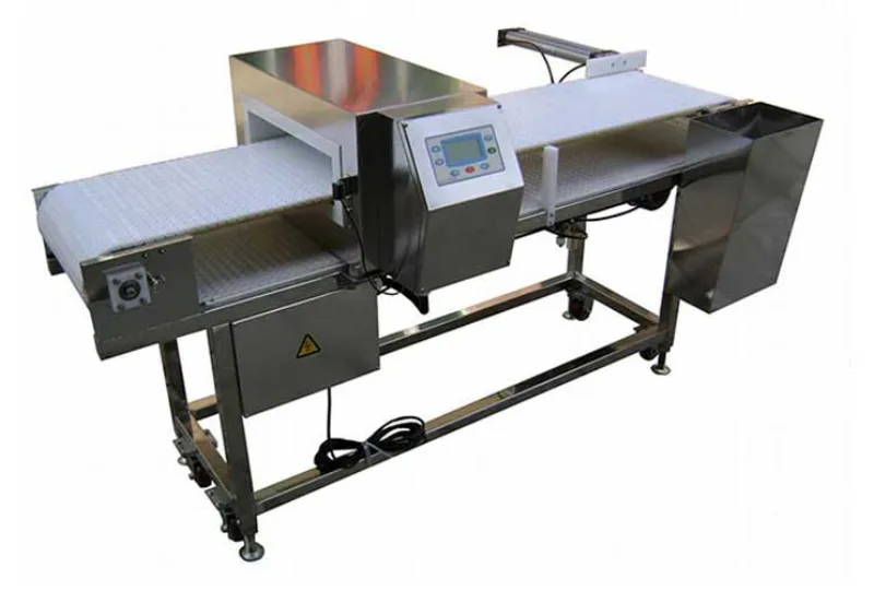
Wafer packaging lines utilize automated material handling systems to transport wafers between different processing stations. These systems employ robotic arms, conveyors, and wafer handling tools to move wafers efficiently and precisely, reducing the risk of damage or contamination. Automation also eliminates manual handling, freeing up operators for more value-added tasks.
High-Precision Alignment
Packaging lines incorporate advanced alignment systems to ensure accurate placement of ICs on substrates. Automated alignment machines use laser or optical sensors to precisely position wafers, ensuring proper interconnections and component placement. This precision alignment minimizes defects and improves the overall yield of functional ICs.
Efficient Die Bonding
Die bonding is the process of attaching the semiconductor die to a substrate, which requires precise and reliable bonding techniques. Wafer packaging lines employ automated die bonders that use advanced bonding technologies, such as eutectic bonding, thermocompression bonding, or flip-chip bonding. These machines ensure strong and durable bonds, preventing device failures and improving product reliability.
Multi-Layer Interconnections
Modern ICs require complex interconnections between multiple layers of conductive materials. Wafer packaging lines use specialized processes to create these interconnections through vias, solder balls, and conductive traces. Automated equipment dispenses solder paste, places solder balls, and performs precision bonding to create multi-layer interconnections that enable high-speed signal transmission and robust device performance.
Encapsulation and Protection
After interconnections, wafers are encapsulated in protective materials to shield them from environmental factors and ensure device reliability. Wafer packaging lines employ automated encapsulation processes, such as molding, overmolding, and conformal coating. These processes create a durable and protective layer around the ICs, enhancing device longevity and preventing damage during handling and storage.
Testing and Quality Control
To ensure the functionality and reliability of packaged ICs, wafer packaging lines incorporate comprehensive testing and quality control measures. Automated testing equipment performs electrical, functional, and environmental tests to identify and eliminate faulty devices. Statistical process control (SPC) systems monitor production processes to identify trends and prevent errors, ensuring consistent product quality.
By implementing these technologies and processes, wafer packaging lines significantly enhance production efficiency in the semiconductor industry. Automation, precision alignment, efficient bonding, multi-layer interconnections, encapsulation, and testing ensure that high-quality ICs are produced in a timely and cost-effective manner, meeting the growing demand for electronic devices.


-
01
How do I choose the right speed for a toas bread packaging line to avoid crushing soft loaves?
22-06-2026 -
 02
02Packaging Machinery: Beyond Sealing, Driving an Efficient, Smart, and Sustainable Future
21-01-2026 -
 03
03Automatic Tray Loading and Packaging Equipment: Boost Efficiency to 160 Bags/Minute
21-11-2025 -
04
Automatic Soap Packaging Machine: Boost Productivity with 99% Qualification Rate
21-11-2025 -
05
A Deep Dive into Automatic Toast Processing and Packaging System
18-11-2025 -
06
The Future of Bakery Production: Automated Toast Processing and Packaging System
18-11-2025 -
07
Reliable Food Packaging Solutions with China Bread, Candy, and Biscuit Machines
11-10-2025 -
08
High-Performance Automated Food Packaging Equipment for Modern Production
11-10-2025 -
09
Reliable Pillow Packing Machines for Efficient Packaging Operations
11-10-2025 -
10
Advanced Fully Automatic Packaging Solutions for Efficient Production
11-10-2025