
The Future of Wafer Packaging Lines- Trends and Innovations
The semiconductor industry is constantly evolving, with new technologies emerging at a rapid pace. As a result, the wafer packaging industry is also undergoing a transformation, as it adapts to meet the demands of new chip designs and technologies. In this article, we will explore the future of wafer packaging lines, examining the key trends and innovations that are shaping this industry.
Advanced Automation and Robotics
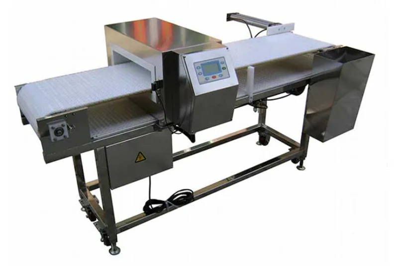
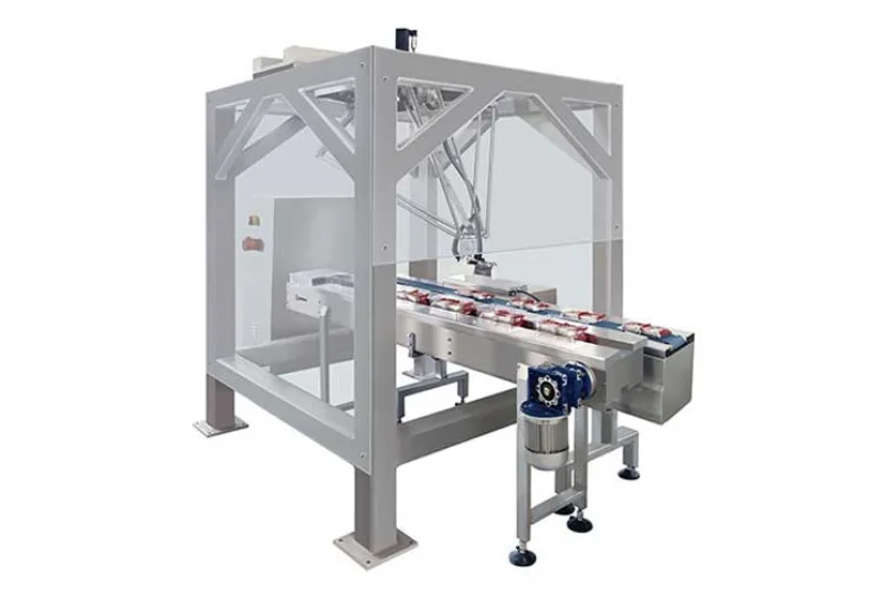
Automation and robotics are playing an increasingly important role in wafer packaging lines. As chips become more complex and packaging requirements become more demanding, manual processes are no longer sufficient to meet production targets. Automated equipment can handle a wide range of tasks, such as die bonding, wire bonding, and encapsulation, with greater precision and efficiency than manual labor. In addition, robots can be programmed to perform repetitive tasks, reducing the risk of errors and improving overall productivity.
Smart and Connected Equipment
The advent of the Internet of Things (IoT) is also having a significant impact on wafer packaging lines. Smart equipment, such as sensors and controllers, can be integrated into the production line to monitor and collect data on various aspects of the process. This data can then be analyzed to identify areas for improvement and optimize production efficiency. Additionally, connected equipment can be remotely monitored and controlled, allowing for real-time adjustments and maintenance to be performed without interrupting production.
Advanced Materials and Technologies
The development of new materials and technologies is also driving innovation in wafer packaging. For example, advanced packaging materials, such as low-k dielectrics and high-density substrates, enable the creation of smaller and thinner packages with improved electrical performance. In addition, new packaging technologies, such as fan-out wafer-level packaging (FOWLP) and system-in-package (SiP), offer unique solutions for integrating multiple chips into a single package.
Integration and Convergence
The wafer packaging industry is also experiencing a trend towards integration and convergence. Companies are increasingly looking to provide end-to-end solutions that encompass wafer fabrication, packaging, and testing. This trend is driven by the need for improved efficiency and control throughout the semiconductor supply chain. In addition, the convergence of different technologies, such as lithography, etching, and packaging, is leading to new and innovative approaches to wafer packaging.
Sustainability and Environmental Considerations
The semiconductor industry is facing increasing pressure to reduce its environmental impact. As a result, wafer packaging lines are being redesigned to be more sustainable. This includes the use of eco-friendly materials and processes, as well as the reduction of energy consumption and waste generation. In addition, some companies are exploring the use of renewable energy sources to power their wafer packaging lines.
Conclusion
The future of wafer packaging lines is bright. As the semiconductor industry continues to evolve, wafer packaging lines will continue to adapt and innovate, meeting the demands of new chip designs and technologies. The trends and innovations discussed in this article are just a few examples of the ways in which the wafer packaging industry is transforming to meet the challenges of the future.


-
01
How do I choose the right speed for a toas bread packaging line to avoid crushing soft loaves?
22-06-2026 -
 02
02Packaging Machinery: Beyond Sealing, Driving an Efficient, Smart, and Sustainable Future
21-01-2026 -
 03
03Automatic Tray Loading and Packaging Equipment: Boost Efficiency to 160 Bags/Minute
21-11-2025 -
 04
04Automatic Soap Packaging Machine: Boost Productivity with 99% Qualification Rate
21-11-2025 -
 05
05A Deep Dive into Automatic Toast Processing and Packaging System
18-11-2025 -
06
The Future of Bakery Production: Automated Toast Processing and Packaging System
18-11-2025 -
 07
07Reliable Food Packaging Solutions with China Bread, Candy, and Biscuit Machines
11-10-2025 -
 08
08High-Performance Automated Food Packaging Equipment for Modern Production
11-10-2025 -
09
Reliable Pillow Packing Machines for Efficient Packaging Operations
11-10-2025 -
 10
10Advanced Fully Automatic Packaging Solutions for Efficient Production
11-10-2025
