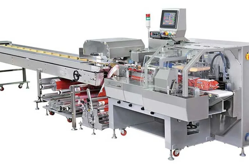
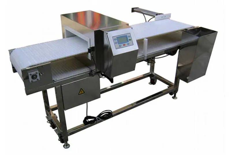
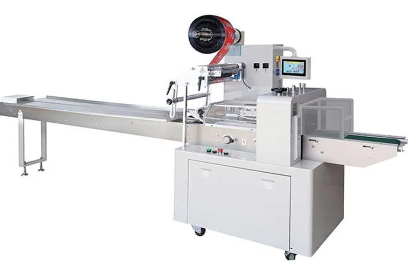
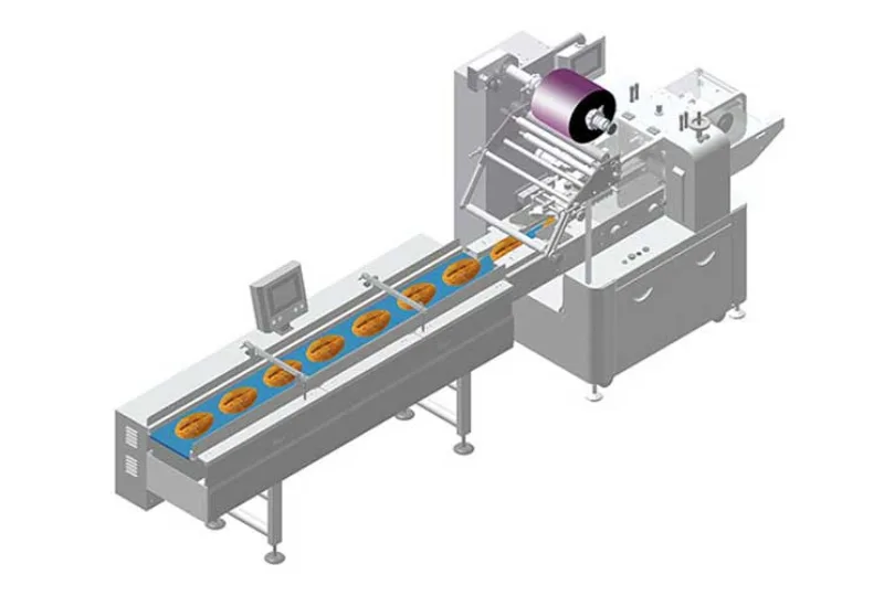
The Technology Behind Wafer Automatic Packaging Machines- How They Work
Introduction:
In the realm of semiconductor manufacturing, precision and efficiency are paramount. Wafer automatic packaging machines stand as the epitome of these virtues, seamlessly combining advanced technologies to ensure the safe and accurate handling of delicate wafers. Join us as we delve into the inner workings of these remarkable machines and uncover the secrets behind their transformative operations.
The Role of Robots and Vision Systems:
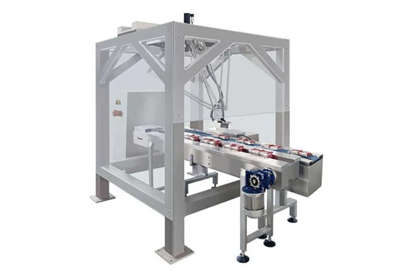
Robots form the backbone of wafer automatic packaging machines, deftly navigating the production environment with unparalleled accuracy. Guided by sophisticated vision systems, these robotic arms precisely pick and place wafers into designated carriers. The vision systems employ advanced algorithms to identify and orient each wafer, ensuring proper alignment throughout the packaging process.
Automated Alignment and Bonding:
At the heart of the packaging process lies the delicate task of bonding the wafers to lead frames. These frames provide electrical connections to the wafers and ensure their stability. Automated alignment systems utilize lasers or other optical techniques to precisely position the wafers with sub-micron accuracy. Subsequently, the bonding process employs advanced adhesives or eutectic alloys to create secure, reliable connections between the wafers and lead frames.
Ultrasonic Welding and Wire Bonding:
Once the wafers are securely bonded to the lead frames, ultrasonic welding takes center stage. These machines generate high-frequency ultrasonic waves that create intense vibrations, causing the lead frame connecting wires to weld with precision. This process ensures the creation of robust electrical connections. Additionally, wire bonding machines employ fine wires to establish electrical pathways between the chip and the lead frame, further enhancing signal integrity.
Testing and Inspection:
To guarantee the reliability and functionality of packaged wafers, a series of rigorous tests are performed. Visual inspection systems scrutinize each package for any physical defects or misalignments. Electrical tests verify the integrity of connections and ensure that the wafers meet stringent performance specifications.
Optimizing Performance Through Machine Learning:
Modern wafer automatic packaging machines incorporate machine learning algorithms to continuously optimize their performance. These algorithms analyze data from the production line, identifying trends and patterns that can improve efficiency and reduce downtime. By continuously learning and adapting, these machines enhance their own operations, setting new benchmarks for productivity and precision.
Conclusion:
Wafer automatic packaging machines represent a technological marvel, combining precision robotics, vision systems, and advanced bonding techniques to deliver unparalleled efficiency and reliability in semiconductor packaging. Through their intricate operations, these machines ensure the safe and accurate handling of delicate wafers, driving innovation and fueling the technological advancements that shape our world. As technology continues to evolve, we can anticipate even more sophisticated and groundbreaking advancements that will further transform the landscape of semiconductor manufacturing.
-
01
Packaging Machinery: Beyond Sealing, Driving an Efficient, Smart, and Sustainable Future
21-01-2026 -
02
Automatic Tray Loading and Packaging Equipment: Boost Efficiency to 160 Bags/Minute
21-11-2025 -
03
Automatic Soap Packaging Machine: Boost Productivity with 99% Qualification Rate
21-11-2025 -
04
A Deep Dive into Automatic Toast Processing and Packaging System
18-11-2025 -
05
The Future of Bakery Production: Automated Toast Processing and Packaging System
18-11-2025 -
06
Reliable Food Packaging Solutions with China Bread, Candy, and Biscuit Machines
11-10-2025 -
07
High-Performance Automated Food Packaging Equipment for Modern Production
11-10-2025 -
08
Reliable Pillow Packing Machines for Efficient Packaging Operations
11-10-2025 -
09
Advanced Fully Automatic Packaging Solutions for Efficient Production
11-10-2025 -
10
Efficient Automatic Food Packaging Solutions for Modern Production
11-10-2025


