The Ultimate Guide to Wafer Packaging Lines
“The Ultimate Guide to Wafer Packaging Lines” is a comprehensive resource that provides an extensive overview of the processes and equipment involved in wafer packaging. It offers a valuable understanding of this critical aspect of semiconductor manufacturing for professionals and students in the field.
Definition and Purpose of Wafer Packaging
Wafer packaging refers to the process of encapsulating semiconductor wafers into protective and functional packages that enable electrical connections and environmental protection. This stage is crucial to ensure the functionality and reliability of integrated circuits (ICs).
Wafer Packaging Process
1. Wafer Preparation
The process begins with wafer preparation, which involves cleaning, thinning, and applying adhesive to the wafer. This prepares the wafer for bonding to the package substrate.
2. Die-Attach and Wire Bonding
Individual dies are attached to the packaging substrate using die-attach materials. Wires are then bonded between the dies and the package terminals.
3. Encapsulation and Molding
The packaged die is covered with molding compound or epoxy resin to provide protection and insulation. The compound is cured using heat and pressure.
Equipment Used in Wafer Packaging
1. Wafer Handling Equipment
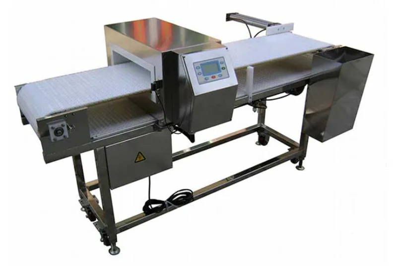
Special equipment is required to handle fragile wafers safely and precisely throughout the packaging process. This includes wafer pick-and-place machines and dicing saws.
2. Die-Attach and Wire Bonding Equipment
Die attachers and wire bonders are used to connect dies to the package substrate. These machines rely on precision motion control and monitoring systems.
Quality Control in Wafer Packaging
Quality control plays a vital role in ensuring the reliability and performance of packaged ICs. Automated optical inspection (AOI), electrical testing, and environmental stress testing are essential to detect and eliminate defects.
Challenges and Trends in Wafer Packaging
Miniaturization, increased I/O count, and the need for higher performance and reliability pose significant challenges in wafer packaging. Advanced packaging technologies such as fan-out wafer-level packaging (FOWLP) and system-in-package (SiP) are being explored to address these challenges.
Conclusion
“The Ultimate Guide to Wafer Packaging Lines” offers a comprehensive exploration of the wafer packaging process, equipment, and quality control measures involved in this critical aspect of semiconductor manufacturing. By providing an in-depth understanding of these topics, the guide serves as an invaluable resource for industry professionals, students, and anyone interested in the intricate world of IC fabrication.


-
01
How do I choose the right speed for a toas bread packaging line to avoid crushing soft loaves?
22-06-2026 -
 02
02Packaging Machinery: Beyond Sealing, Driving an Efficient, Smart, and Sustainable Future
21-01-2026 -
 03
03Automatic Tray Loading and Packaging Equipment: Boost Efficiency to 160 Bags/Minute
21-11-2025 -
04
Automatic Soap Packaging Machine: Boost Productivity with 99% Qualification Rate
21-11-2025 -
05
A Deep Dive into Automatic Toast Processing and Packaging System
18-11-2025 -
06
The Future of Bakery Production: Automated Toast Processing and Packaging System
18-11-2025 -
07
Reliable Food Packaging Solutions with China Bread, Candy, and Biscuit Machines
11-10-2025 -
08
High-Performance Automated Food Packaging Equipment for Modern Production
11-10-2025 -
09
Reliable Pillow Packing Machines for Efficient Packaging Operations
11-10-2025 -
10
Advanced Fully Automatic Packaging Solutions for Efficient Production
11-10-2025